Semiconductors

ADVANCED SOLUTIONS FOR THE SEMICONDUCTOR INDUSTRY

Our world-leading range of high-quality CVD, grits and machining products provide solutions to customers across multiple stages of the semiconductor and consumer electronics value chains

Semiconductors are critical enablers at the heart of today’s GPUs, HPC, AI accelerators and advanced CPUs that power smartphones, servers and hyperscale datacenters. Innovations in semiconductor design and manufacturing underpin disruptive technologies such as 5G and 6G, the internet of things (IoT), artificial intelligence (AI), electric vehicles (EV), and advanced defense and security applications.

Element Six’s portfolio spans from chemical vapour deposition (CVD) diamond and composite solutions for RF power devices to drop in copper diamond components for GPU and AI accelerator thermal management in datacenter servers.

Our CVD diamond thermal management solutions improve the reliability of mission-critical, high-power density RF amplifiers, and enable testing and inspection of processed wafers and semiconductor chips. Our high-performance diamond grits, powders and wire drawing die are integral to the cutting and polishing of semiconductor wafers and the hard optical materials used in smart electronics. Device assembly and integration require precision machining of printed circuit boards and a variety of metal, glass and ceramic materials - our single crystal and polycrystalline diamond ranges for precision machining tools provide the quality and reliability expected by the world-leading industrial manufacturers of consumer electronics.

With a wide range of synthetic diamond solutions, decades of technical expertise, scale capabilities, and a collaborative approach to material development, Element Six is uniquely equipped to enable semiconductor manufacturers to optimise their products and overcome even their most demanding process challenges.

Key application areas

Our innovation and production capabilities deliver synthetic diamond solutions that generate value and competitive advantage at critical stages of the semiconductor manufacturing value chain.

View our brochures

Find out the specific details of the performance of our supermaterials and how they apply to your industry:

Browse our world-leading diamond solutions

Buy a sample of our award-winning synthetic diamond materials on our webstore

THERMAL MANAGEMENT

The performance requirements of today’s semiconductor devices and their manufacturing tools require advanced solutions to manage heat fluxes beyond the capabilities of conventional materials.

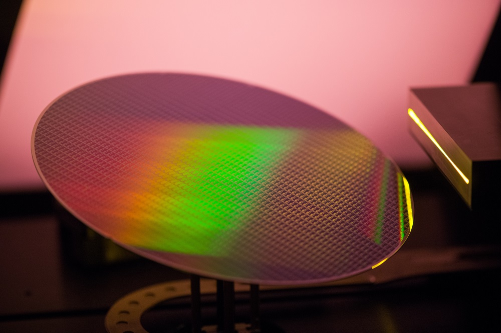
CVD diamond heat spreaders and optical windows eliminate heat flux bottlenecks in high power devices, from GaN RF power amplifiers to chiplet-based GPUs and AI accelerators with HBM memory, while in conjunction optimising wafer fabrication and inspection tools. Discover WSC™ wafer single crystal synthetic diamond solutions for improved system performance and device life and explore diamond baseplates and thermal coins for GPU chiplets and AI accelerator modules.

Access our dedicated WSC™ brochure to learn more.

Thermal management

Materials processing

Semiconductor production consists of a complex chain of fabrication and processing stages in which the minimisation of manufacturing defects is paramount.

Our diamond grit, micron and fine micron are engineered to produce highly consistent properties and behaviours, taking the unpredictability out of the critical dicing, lapping and polishing steps.

Materials processing

Precision machining

Today’s consumer electronic products combine disruptive technology and innovative design. For manufacturers, this means novel materials with demanding machining requirements.

Element Six’s polycrystalline and single crystal diamond ranges match the needs of toolmakers, delivering the ultimate solution in terms quality, consistency, and precision finish.

Precision machining

Diamond substrates

Electronic grade CVD diamond has a low dielectric constant, high charge collection efficiency and is radiation hard, making it an ideal material for high energy particle detectors.

In addition, its high breakdown field and excellent carrier transport properties are attracting increased interest for next generation high-power field effect transistors.

These same properties also make diamond substrates a compelling long term thermal platform beneath future CPU/GPU chiplets and AI accelerators, where bringing diamond closer to the junction is key to overcoming the thermal limits of advanced packaging.

Diamond substrates